
Semiconductor production is dependent upon specialized elements to handle precision and high quality. Those elements permit important processes within sealed environments.
One crucial component lets in visible tracking whilst holding chambers completely sealed. This twin serve as helps each statement and effort transmission wishes.
More than a few stainless-steel and glass fabrics meet other operational necessities. The suitable subject material selection guarantees sturdiness and optimum functionality.
This how-to information explores the sensible programs of those elements. We’ll read about their function throughout other semiconductor production phases.
Correct variety at once affects procedure potency and ultimate product high quality. Working out those programs is helping optimise production results.
Key Takeaways
- Specialized viewports handle seal integrity whilst enabling visible get entry to
- They serve twin functions: procedure statement and effort transmission
- Subject material variety varies by way of particular semiconductor utility wishes
- Correct part selection impacts production potency and yield high quality
- Other production phases require particular viewport traits
- Stainless-steel and high quality glass are not unusual building fabrics
- Working out programs is helping optimise semiconductor manufacturing processes
Working out Vacuum Viewports and Their Position in Semiconductor Gear
Statement elements supply a very powerful visibility into differently inaccessible production processes.
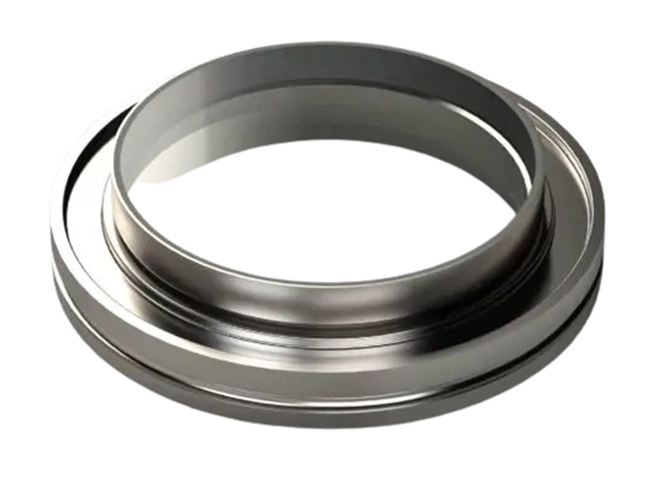
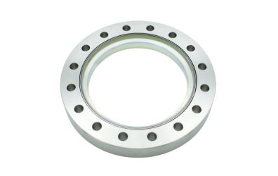
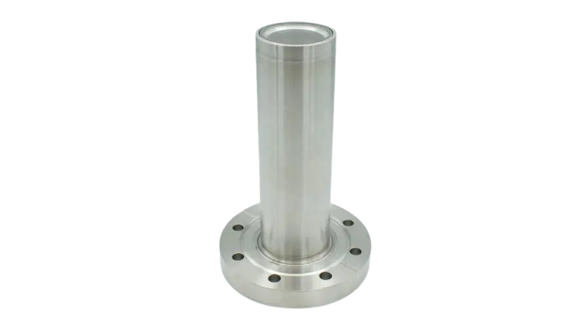
Those specialized optical home windows handle entire environmental isolation. They use complex airtight sealing ways to maintain chamber integrity.
3 number one purposes outline the aim of vacuum viewports in semiconductor apparatus. First, they permit visible tracking of inner processes. 2nd, they permit illumination of the chamber inner. 3rd, they transmit quite a lot of power paperwork to have an effect on processes.
More than a few semiconductor production equipment utilise those elements. Etching methods, deposition apparatus, and implantation equipment all require visible get entry to issues. Each and every utility has particular subject material and design necessities.
| Chamber Dimension Vary | Standard Packages | Viewport Necessities |
| 10-50 cm | Analysis & Building | Small diameter, elementary sealing |
| 50-200 cm | Pilot Manufacturing | Medium dimension, enhanced sturdiness |
| 200+ cm | Complete-scale Production | Massive structure, top class fabrics |
| Distinctiveness (e.g., 122 toes) | Analysis Amenities | Customized engineering, excessive specs |
Semiconductor processes function below other force stipulations. Prime vacuum environments in most cases vary from 10⁻³ to ten⁻⁷ torr. Extremely-high vacuum methods achieve pressures beneath 10⁻⁹ torr.
Laser programs constitute some other important use case. Optical tracking methods depend on transparent transmission paths. Power supply for procedure amendment calls for exact optical elements.
Outgassing charges considerably have an effect on semiconductor production high quality. Low-outgassing fabrics save you contamination of delicate processes. Correct subject material variety guarantees minimum particulate technology.
Actual-world examples come with plasma etching statement and deposition fee tracking. Those programs exhibit the sensible significance of visible get entry to elements. Procedure engineers depend on them for high quality keep an eye on and troubleshooting.
Subject material alternatives range by way of particular utility wishes. Glass choices supply superb optical readability. Metal choices be offering enhanced sturdiness for tough environments.
Deciding on the Proper Viewport Subject material for Semiconductor Packages
Subject material variety paperwork the root of optical part functionality in semiconductor equipment. The proper selection guarantees each visible readability and chamber integrity right through production processes.
Other fabrics be offering distinctive benefits for particular programs. Working out those homes is helping optimise semiconductor manufacturing results.
| Subject material Sort | Transmission Vary | Max Bake Temperature | Number one Packages |
| Borosilicate Glass | Visual spectrum | 200°C | Common statement, plasma tracking |
| Fused Silica (Quartz) | UV to DUV | 200°C | Laser methods, precision optics |
| Sapphire | UV to NIR | 450°C | Prime-temperature processes |
| Zinc Selenide | Infrared | 150°C | Thermal imaging, IR programs |
| Magnesium Fluoride | VUV to mid-IR | 250°C | Vast spectrum programs |
| Calcium Fluoride | VUV to IR | 300°C | Laser-resistant environments |
Borosilicate glass supplies superb visual gentle transmission with minimum distortion. Its thermal surprise resistance makes it appropriate for quite a lot of semiconductor environments.
Fused silica, sometimes called quartz, gives exceptional UV transmission functions. This subject material kind excels in precision optics and laser programs.
Sapphire delivers outstanding sturdiness throughout excessive stipulations. Its extensive transmission vary covers ultraviolet to near-infrared spectra.
Infrared programs ceaselessly have the benefit of zinc selenide elements. This subject material supplies excessive IR transmission for thermal tracking methods.
Magnesium fluoride covers an exceptionally extensive spectral vary. From vacuum ultraviolet to mid-infrared, it maintains constant functionality.
Calcium fluoride gives the broadest transmission functions amongst not unusual fabrics. It combines chemical resistance with laser harm tolerance.
Thermal homes considerably affect subject material variety. Most bake temperatures resolve suitability for high-temperature processes.
Chemical resistance proves a very powerful in competitive semiconductor environments. Procedure gases and cleansing brokers can degrade incompatible fabrics.
Mechanical sturdiness varies significantly between subject material varieties. Scratch resistance impacts long-term functionality and upkeep necessities.
Value-performance tradeoffs require cautious attention. Top class fabrics like sapphire justify funding in important programs.
Laser programs call for particular optical traits. Precision necessities come with minimum absorption and scatter homes.
Environmental elements information ultimate subject material variety. Temperature fluctuations, force stipulations, and chemical publicity all affect alternatives.
Actual-world examples exhibit sensible subject material programs. Lithography methods in most cases use fused silica for its DUV transmission.
Etching chambers ceaselessly make use of borosilicate glass for plasma statement. Deposition equipment would possibly require sapphire for high-temperature visibility.
Correct subject material variety at once affects production potency. The suitable selection reduces downtime and improves procedure keep an eye on.
High quality issues come with outgassing charges and particulate technology. Low-contamination fabrics maintain delicate semiconductor processes.
Customized coatings can make stronger base subject material functionality. Anti-reflective therapies toughen transmission for particular wavelength levels.
Software-specific necessities will have to force subject material selections. Matching subject material homes to procedure wishes guarantees optimum effects.
- Evaluation transmission wishes throughout UV, visual, and IR spectra
- Believe thermal necessities together with bake temperatures
- Assess chemical compatibility with procedure environments
- Stability mechanical sturdiness towards value constraints
- Think about precision wishes for laser and optical methods
- Evaluate environmental stipulations and publicity dangers
Subject material science continues advancing semiconductor functions. New compositions be offering progressed functionality for rising programs.
Key Specs for Semiconductor Vacuum Viewports
Technical specs at once resolve the operational functions of optical get entry to elements. Those detailed necessities be sure that dependable functionality throughout numerous semiconductor production environments.
Bakeout temperature specs range considerably by way of subject material and building. Usual CF/KF flange configurations in most cases take care of 150°C, whilst O-rings prolong this vary to 250°C. Quartz fabrics resist 200°C, and sapphire elements tolerate excessive temperatures as much as 450°C.
Thermal gradient boundaries save you pressure fractures all over temperature adjustments. Usual elements take care of 25°C according to minute, whilst uniqueness fabrics require slower 20°C according to minute charges. Top class merchandise want cautious 3°C according to minute ramping.
Transmission functionality spans a couple of wavelength levels with other potency ranges. Broadband anti-reflection coatings on quartz reach outstanding 99% potency in particular spectral bands.
Those coating choices come with each single-layer and multi-layer BBAR configurations. Each and every coating kind optimises functionality for specific wavelength programs. Correct coating variety maximizes power transmission whilst minimizing mirrored image losses.
Flange subject material alternatives come with 304 stainless-steel for common programs. Extra tough environments would possibly require 316LN stainless-steel or titanium choices. Each and every subject material gives distinct benefits for particular operational stipulations.
Outgassing fee specs turn out important for ultra-high vacuum semiconductor programs. Low outgassing fabrics save you contamination of delicate production processes. This specification at once affects ultimate product high quality and yield charges.
Dimension and dimensional necessities range by way of chamber configuration and alertness wishes. Usual sizes accommodate maximum manufacturing apparatus, whilst customized dimensions serve specialized analysis amenities. Correct sizing guarantees optimum integration with current methods.
Force score specs relate at once to subject material alternatives and building high quality. Upper scores in most cases require top class fabrics and enhanced sealing applied sciences. Those scores be sure that protection and reliability below operational stipulations.
High quality keep an eye on requirements practice stringent UHV production protocols. Cleansing procedures do away with particulate contamination that would have an effect on semiconductor processes. ISO 9001:2015 certification guarantees constant high quality throughout manufacturing batches.
Those complete specs shape the root for part variety. Working out each and every parameter is helping optimise semiconductor production results. Correct specification matching guarantees long-term reliability and procedure consistency.
Enforcing Vacuum Viewports in Particular Semiconductor Processes
Semiconductor fabrication calls for exact part integration throughout numerous production phases. Each and every procedure calls for adapted optical get entry to answers to handle high quality and potency.
Lithography methods have the benefit of fused silica elements. Those fabrics supply remarkable deep ultraviolet transmission for trend switch accuracy.
Etching chambers provide difficult corrosive environments. Sapphire and calcium fluoride fabrics resist competitive chemical publicity whilst keeping up visibility.
Those powerful choices save you clouding and degradation all over plasma etching operations. Their chemical resistance guarantees constant functionality over prolonged classes.
Deposition methods function at increased temperatures. Prime-temperature viewports handle seal integrity whilst permitting procedure statement.
Thermal processing programs require particular transmission traits. Infrared-compatible fabrics permit correct temperature tracking and keep an eye on.
Metrology methods call for remarkable optical readability. Precision transmission guarantees correct size and inspection effects.
Laser processing programs want specialized elements. Calcium fluoride gives superb laser harm resistance for trimming operations.
Cleanroom set up calls for meticulous contamination keep an eye on. Correct dealing with procedures save you particulate creation all over part integration.
Integration with pumping methods wishes cautious making plans. Force tracking apparatus connects seamlessly with correctly specified viewports.
Coating variety varies by way of particular utility wishes. Anti-reflective therapies optimise functionality for specific wavelength levels.
Unmarried-layer coatings swimsuit particular laser wavelengths. Broadband choices quilt wider spectral levels for multi-purpose programs.
Those implementation issues be sure that optimum functionality throughout other semiconductor processes. Correct variety at once affects production yield and high quality.
Actual-world luck tales exhibit sensible implementation advantages. One foundry progressed yield by way of 3% via optimised viewport variety.
Some other producer decreased downtime by way of imposing sapphire viewports in etching equipment. Their enhanced sturdiness withstood competitive cleansing cycles.
Complicated coating applied sciences proceed evolving to satisfy new demanding situations. Rising programs call for more and more subtle optical answers.
Correct implementation follows established best possible practices whilst permitting customisation. Each and every semiconductor procedure has distinctive necessities that information ultimate variety.
Set up and Upkeep Highest Practices
Correct dealing with guarantees optical elements serve as appropriately in semiconductor equipment. Following pointers prevents harm and maintains chamber integrity.
Set up starts with cautious unpacking. All the time put on blank gloves to give protection to surfaces. Check out elements for delivery harm ahead of continuing.
Other flange varieties require particular set up approaches. Each and every connection taste has distinctive sealing traits and torque necessities.
| Flange Sort | Torque Specification | Seal Subject material | Temperature Prohibit |
| CF (ConFlat) | 120-140 in-lbs | Copper gasket | 450°C |
| KF (Fast Flange) | 60-80 in-lbs | Viton O-ring | 200°C |
| ISO | 90-110 in-lbs | Kalrez O-ring | 250°C |
| Customized Flanges | In step with producer | More than a few choices | Varies |
Cleansing follows strict UHV protocols. Use best licensed solvents and lint-free wipes. Steer clear of touching optical surfaces all over cleansing.
Upkeep schedules rely on operational depth. Prime-use methods want per month inspections. Low-use programs would possibly require quarterly tests.
O-ring substitute follows particular pointers. A few of these rings are appropriate for high-temperature programs as much as 250°C. All the time use manufacturer-specified substitute portions.
Bakeout procedures require cautious temperature keep an eye on. The utmost heating fee will have to now not exceed 3°C according to minute. This prevents thermal pressure harm.
Leak detection makes use of helium mass spectrometry. Common trying out guarantees chamber integrity. Record all check effects for high quality information.
Protection protocols give protection to each body of workers and kit. All the time depressurise methods ahead of repairs. Use right kind lifting apparatus for heavy elements.
Demountable designs permit substrate removing for cleansing. This selection simplifies repairs with out breaking seals. It additionally allows customized coating upgrades.
Recessed zero-profile designs be offering most coverage. They supply extensive viewing angles whilst shielding optical surfaces. This design reduces contamination dangers.
High quality keep an eye on groups test each and every product ahead of cargo. They be sure that compliance with semiconductor business requirements. This contains cleanliness and function trying out.
Documentation maintains compliance with high quality methods. Stay detailed information of all repairs actions. Come with set up dates, inspections, and replacements.
Troubleshooting not unusual problems calls for systematic means. Maximum issues relate to wrong set up or broken seals. Practice producer pointers for solution.
Correct set up and upkeep prolong part lifespan. In addition they be sure that constant production high quality. Following best possible practices reduces downtime and prices.
Optimising Your Semiconductor Vacuum Viewport Variety
Clever part variety at once influences semiconductor production results and yield charges. The suitable alternatives steadiness functionality necessities with financial issues throughout other manufacturing scales.
Subject material optimisation comes to cautious research of transmission wishes and environmental stipulations. Customized coatings make stronger functionality for particular wavelength levels whilst decreasing mirrored image losses.
Long run-proofing calls for making an allowance for evolving era calls for and scalability wishes. Partnering with skilled providers guarantees get entry to to skilled recommendation and customized answers.
Overall value research will have to come with repairs necessities and long-term reliability elements. Efficiency benchmarking towards business requirements is helping validate variety selections for important semiconductor programs.


